In the past decade, optical sensing tasks have become more demanding. As a result, it has become critical to build miniaturized, inexpensive sensors that can be integrated on-chip to enable mobile applications in smart phones, autonomous vehicles, robots, and drones. Also, algorithms are increasingly important in sensing, and many recent developments have utilized machine-learning algorithms.

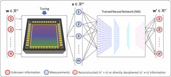
Schematic of geometric deep optical sensing. Image credit: Yale University
In a new paper in Science, researchers in the lab of Prof. Fengnian Xia in Electrical Engineering introduce a new concept they call “Geometric Optical Deep Sensing” for sensing and imaging.
The concept, which leverages innovations in device technology, condensed matter physics and deep learning, has the potential to move away from hardware-oriented approaches to software-oriented ones.
The paper was authored with collaborators at University of Texas, Bar-Ilan University of Israel and Vienna University of Technology of Austria. In this new concept, “geometric” indicates that the sensor outputs consist of multi-element data, which can be viewed as points in high dimensional vector spaces. “Deep” highlights the critical role of deep neural networks in this sensing scheme.
Shaofan Yuan, a former Ph.D. student in Xia’s lab and co-lead author of the paper, noted that conventional optical sensing requires multiple optical devices to fully capture the unknown properties of the light beam. These include different devices to measure the intensity, polarization, wavelengths, and the spatial distribution of the light. All these devices add up and make for a bulky and expensive system.
“Much effort has been made to make optical sensing devices compact and multifunctional in the past, and advanced machine learning algorithms have accelerated optical sensing solutions using miniatursed devices,” said Yuan, who added that future optical sensing technologies will be a highly interdisciplinary field.
“This field will benefit from innovations in device structures, demonstrations of emerging optical and optoelectronic phenomena, and advancement in machine-learning algorithms.”
Chao Ma, a PhD student in Xia’s lab and the other co-lead author, noted that device reconfigurability is key to achieving complicated optical sensing with a single device.

Among the existing projects reviewed is an intelligent sensing process previously developed by the Xia group: quantum geometric properties determine the photo responses, which are then interpreted by a neural network. Image credit: Xia group
“A single reconfigurable device that can be operated at different states is essential to generate a multi-element photoresponse data capturing multiple unknown properties of light sometimes in an implicit manner, and then machine-learning algorithms can be used to interpret the data,” Ma said.
The scheme involves using reconfigurable sensors and deep neural networks for the information encoding/decoding processes.
The networks have been trained with known properties of light and can extract the right information from the multi-element outputs of reconfigurable sensors. Xia notes that it interprets the multi-element photoresponses like image recognition programs.
“If you want it to recognize an image, whether it’s a dog or cat or human beings or cars, you collect numerous photos with known information, then train it,” he said.
“Then we just give the neural network an unknown figure, and that will tell you. The similar idea is used here.”
The researchers noted that the underlying principle of the scheme applies not just to light but other areas – for instance, for sensing magnetic fields. Xia said he and his collaborators are currently looking at potential applications. One possibility is using such integrated sensing devices to make autonomous vehicles safer.
Source: Yale University


